4A_LA_DECOUVERTE_DE_LELECTRONIQUE t etoile
4Electronique - Les Composants De L'électronique De Puissance eto
Electronique - Les Composants De L'électronique De Puissance e1.
Electronic Symbols
CIRCUIT SYMBOLS
7ELECTRONIQUE3
15Hachette Physique Chimie Terminale S livre du professeur spécifique partie 1 etoile
Circuit_Analysis_3E etoile etoile
ELECTRICS AND ELECTRONICS
AIDE-MEMOIRE TRAITEMENT DU SIGNAL
TRAITEMENT NUMERIQUE DU SIGNAL
MAXI FICHES ELECTRONIQUE
PHYSIQUE DES SEMICONDUCTEURS ET DES COMPOSANTS ELECTRONIQUES
ELECTRONIQUE DE A à Z
L'ELECTRONIQUE PAR L'EXPERIENCE
INTRODUCTION A L'ELECTRONIQUE ANALOGIQUE
ELECTRONIQUE NUMERIQUE EN 26 FICHES
ELECTRONIQUE APPLIQUEE AUX HAUTES FREQUENCES
AIDE-MEMOIRE ELECTRONIQUE
AIDE-MEMOIRE ELECTRONIQUE ANALOGIQUE ET NUMERIQUE
Électronique-Principes et Applications :
A la découverte de l'électronique :
Électronique de A a Z :
Aide Mémoire électronique
Construisez votre émetteur FM
Micro et nano-électronique :
L'électronique par l’expérience:
Trésors de Physique Chimie - Collections pdf ebooks à télécharger gratuitement
Electronique : Filtre RL actif.
Electronique : Filtre passe-bande.
Electronique : FILTRE DE SALLEN-KEY SIMPLIFIE.
Electronique : CIRCUIT DE FILTRE A BASE AOP.
Electronique : CIRCUIT DE FILTRE A BASE AOP BIS.
Electronique : CIRCUIT DE FILTRE A BASE AOP.
Electronique : CIRCUIT DE FILTRE A BASE AOP BIS.
Electronique : FILTRE DE SALLEN-KEY SIMPLIFIE.
Electronique : Filtre passe-bande.
Electronique : Filtre RL actif.
SEMICONDUCTOR
Electronic and Optoelectronic Properties of Semiconductor Structures - singh
127 An overview of how semiconductor bandstructure influences device performance
236 Auger coefficients of some semiconductors.
231 Breakdown electric fields in some materials
447 Electro-optic coefficients for some materials
-------------------------------------------------------------------------------------------------------------------
-------------------------------------------------------------------------------------------------------------------
-------------------------------------------------------------------------------------------------------------------
-------------------------------------------------------------------------------------------------------------------
288 Bandgaps along with electron and hole mobilities in several semiconductors
384 Values of Ep for different semiconductors
-------------------------------------------------------------------------------------------------------------------
-------------------------------------------------------------------------------------------------------------------
J. Singh, Electronic and Optoelectronic Properties of Semiconductor Structures, Cambridge University Press, 2003. https://books.google.fr/books?id=HWJmngEACAAJ. Page 127; 236; 231; 447; 228; 384.
-------------------------------------------------------------------------------------------------------------------
-------------------------------------------------------------------------------------------------------------------
Thin Film Materials Technology
201 Thin Film Materials and Applications
-------------------------------------------------------------------------------------------------------------------
-------------------------------------------------------------------------------------------------------------------
-------------------------------------------------------------------------------------------------------------------
-------------------------------------------------------------------------------------------------------------------
K. Wasa, M. Kitabatake, H. Adachi, Thin Film Materials Technology: Sputtering of Compound Materials, Elsevier Science, 2004. https://books.google.fr/books?id=pmpV4RYHpdcC. Page 201.
Solar Energy Conversion
209 Schottky junction barrier energies (eV)
85 The square of the intrinsic carrier concentration
83-91 Electrons and Holes
103 ELECTRON AND HOLE LIFE TIME
94-95 Electron hole mobility
-------------------------------------------------------------------------------------------------------------------
-------------------------------------------------------------------------------------------------------------------
-------------------------------------------------------------------------------------------------------------------
-------------------------------------------------------------------------------------------------------------------
103 ELECTRON AND HOLE LIFE TIME
-------------------------------------------------------------------------------------------------------------------
-------------------------------------------------------------------------------------------------------------------
-------------------------------------------------------------------------------------------------------------------
------------------------------------------------------------------------------------------------------------------- 94-95 Electron hole mobility
-------------------------------------------------------------------------------------------------------------------
-------------------------------------------------------------------------------------------------------------------
-------------------------------------------------------------------------------------------------------------------
------------------------------------------------------------------------------------------------------------------- 145-148 Reflection and Absorption The electrical power density, Limit Thickness
-------------------------------------------------------------------------------------------------------------------
-------------------------------------------------------------------------------------------------------------------
-------------------------------------------------------------------------------------------------------------------
------------------------------------------------------------------------------------------------------------------- 122 The reflection coefficient, f
-------------------------------------------------------------------------------------------------------------------
-------------------------------------------------------------------------------------------------------------------
-------------------------------------------------------------------------------------------------------------------
------------------------------------------------------------------------------------------------------------------- 130 Energy gap values and Refractive Index
-------------------------------------------------------------------------------------------------------------------
-------------------------------------------------------------------------------------------------------------------
-------------------------------------------------------------------------------------------------------------------
------------------------------------------------------------------------------------------------------------------- A. R.C. Neville, Solar Energy Conversion: The Solar Cell, Elsevier Science, 1995. https://books.google.fr/books?id=B1Gbvn0uhdYC. Page 209; 85; 83-91; 103; 94-95; 145-148; 122; 130.
Wiley - Physics of Semiconductor Devices
501 Comparison of Semiconductor Materials for Power Applications
467 Semiconductor Materials Related to Transferred-Electron Effect at 300 K
-------------------------------------------------------------------------------------------------------------------
-------------------------------------------------------------------------------------------------------------------
-------------------------------------------------------------------------------------------------------------------
------------------------------------------------------------------------------------------------------------------- 184-186 Measured Barrier Heights
-------------------------------------------------------------------------------------------------------------------
-------------------------------------------------------------------------------------------------------------------
-------------------------------------------------------------------------------------------------------------------
------------------------------------------------------------------------------------------------------------------- 737-740 Physical Constants and Properties of Si and GaAs
-------------------------------------------------------------------------------------------------------------------
-------------------------------------------------------------------------------------------------------------------
-------------------------------------------------------------------------------------------------------------------
-------------------------------------------------------------------------------------------------------------------
S.M. Sze, K.K. Ng, Physics of Semiconductor Devices, Wiley, 2006. https://books.google.fr/books?id=o4unkmHBHb8C. Page 501; 184-186;737-740.
Advanced-semiconductor-fundamentals-se-robert-f-pierret
9-13 Basic Semiconductor Properties
121 Concentration parameter
104 Density of states effectives masses for Ge, Si, GaAs
89-91 Electron hole effective masses
-------------------------------------------------------------------------------------------------------------------
-------------------------------------------------------------------------------------------------------------------
-------------------------------------------------------------------------------------------------------------------
------------------------------------------------------------------------------------------------------------------- 89-91 Electron hole effective masses
-------------------------------------------------------------------------------------------------------------------
-------------------------------------------------------------------------------------------------------------------
-------------------------------------------------------------------------------------------------------------------
-------------------------------------------------------------------------------------------------------------------
A. R.F. Pierret, Semiconductor Device Fundamentals, Addison-Wesley, 1996. https://books.google.fr/books?id=GMZFHwAACAAJ. Page 9-13, 121, 104, 89-91.
Semiconductor Physics And Devices 3rd ed. - J. Neamen
132 Effective density of states and Values of ni
-------------------------------------------------------------------------------------------------------------------
-------------------------------------------------------------------------------------------------------------------
-------------------------------------------------------------------------------------------------------------------
-------------------------------------------------------------------------------------------------------------------
178 Typical Mobility Values at T=300K and low doping concentrations
-------------------------------------------------------------------------------------------------------------------
------------------------------------------------------------------------------------------------------------------- 141-142 Impurity ionization energies in silicon, germanium and Gallium arsenide
-------------------------------------------------------------------------------------------------------------------
-------------------------------------------------------------------------------------------------------------------
-------------------------------------------------------------------------------------------------------------------
------------------------------------------------------------------------------------------------------------------- 199 Typical mobility and diffusion coefficient values at T=300K
-------------------------------------------------------------------------------------------------------------------
-------------------------------------------------------------------------------------------------------------------
-------------------------------------------------------------------------------------------------------------------
------------------------------------------------------------------------------------------------------------------- A. D.A. Neamen, Semiconductor physics and devices: basic principles, McGraw-Hill, 2003. https://books.google.fr/books?id=TPE9AQAAIAAJ. Page 132; 178; 141-142; 199.
2100516434semiconducteurs
31;37;39 Energie du gap des différents semiconducteurs
-------------------------------------------------------------------------------------------------------------------
-------------------------------------------------------------------------------------------------------------------
-------------------------------------------------------------------------------------------------------------------
-------------------------------------------------------------------------------------------------------------------
H. Mathieu, H. Fanet, Physique des semiconducteurs et des composants électroniques - 6ème édition: Cours et exercices corrigés, Dunod, 2009. https://books.google.fr/books?id=vAXJsXS0yosC. Page 31;37;39.
-----------------------------------------------------------------------------------------
Reference Data for Engineers
660 PROPERTIES OF SEMICONDUCTOR MATERIAL (300 K)
-------------------------------------------------------------------------------------------------------------------
-------------------------------------------------------------------------------------------------------------------
-------------------------------------------------------------------------------------------------------------------
-------------------------------------------------------------------------------------------------------------------
M.E. Van Valkenburg, W.M. Middleton, Reference Data for Engineers: Radio, Electronics, Computers and Communications, Elsevier Science, 2002. https://books.google.fr/books?id=R67HARlhisYC. Page 660.
--------------------------
Thin Film Solar Cells- Fabrication, Characterization and Applications
282 Shallow dopants in CdTe
-------------------------------------------------------------------------------------------------------------------
-------------------------------------------------------------------------------------------------------------------
-------------------------------------------------------------------------------------------------------------------
-------------------------------------------------------------------------------------------------------------------
J. Poortmans, V. Arkhipov, Thin Film Solar Cells: Fabrication, Characterization and Applications, Wiley, 2006. https://books.google.fr/books?id=SvVYBK6YAxAC. Page 282.
-----------------------------------------------------------------
Claus F. Klingshirn Semiconductor Optics 4th ed. - 2012
199-203; 585 An Overview of Semiconducting Materials
-------------------------------------------------------------------------------------------------------------------
-------------------------------------------------------------------------------------------------------------------
-------------------------------------------------------------------------------------------------------------------
-------------------------------------------------------------------------------------------------------------------
C.F. Klingshirn, Semiconductor Optics, Springer Berlin Heidelberg, 2012. https://books.google.fr/books?id=Jwl6v3JGxaYC. Page 199-203; 585.
----------------------------------------------------------------------------------------------------------
Electrochemistry of semiconductors and electronics.. processes and devices
196 Properties of Candidate Semiconductors
-------------------------------------------------------------------------------------------------------------------
-------------------------------------------------------------------------------------------------------------------
-------------------------------------------------------------------------------------------------------------------
-------------------------------------------------------------------------------------------------------------------
J. McHardy, F. Ludwig, Electrochemistry of semiconductors and electronics: processes and devices, Noyes Publications, 1992. https://books.google.fr/books?id=uWBwAAAAIAAJ. Page 196.
------------------------------
Luminescent Materials and Applications
40 Band gap and Bohr radii data for selected semiconductor
-------------------------------------------------------------------------------------------------------------------
-------------------------------------------------------------------------------------------------------------------
-------------------------------------------------------------------------------------------------------------------
-------------------------------------------------------------------------------------------------------------------
A. Kitai, Luminescent Materials and Applications, Wiley, 2008. https://books.google.fr/books?id=yLy07tnBZ90C. Page 40.
------------------------
PROCEDE DE DEPOT DE COUCHE MINCE
Nanostructured Materials for Advanced Technological Applications
422 Cross section of an MBE
-------------------------------------------------------------------------------------------------------------------
-------------------------------------------------------------------------------------------------------------------
-------------------------------------------------------------------------------------------------------------------
-------------------------------------------------------------------------------------------------------------------
J. Reithmaier, P. Petkov, W. Kulisch, C. Popov, Nanostructured Materials for Advanced Technological Applications, Springer Netherlands, 2009. https://books.google.fr/books?id=_iSdAv8_yGUC. Page 422.
Electronic and Optoelectronic Properties of Semiconductor Structures - singh
25-34 CRYSTAL GROWTH
-------------------------------------------------------------------------------------------------------------------
-------------------------------------------------------------------------------------------------------------------
-------------------------------------------------------------------------------------------------------------------
-------------------------------------------------------------------------------------------------------------------
J. Singh, Electronic and Optoelectronic Properties of Semiconductor Structures, Cambridge University Press, 2003. https://books.google.fr/books?id=HWJmngEACAAJ. Page 24-35.
-------------------------------------------------------
Thin Film Materials Technology
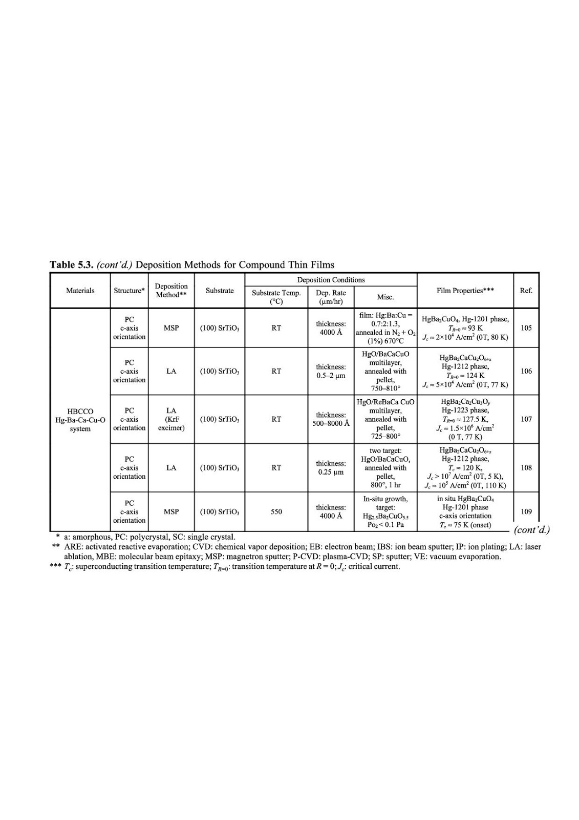
200-227 Deposition Methods for Compound Thin Films
-------------------------------------------------------------------------------------------------------------------
-------------------------------------------------------------------------------------------------------------------
-------------------------------------------
-----------------------------------------
-------------------------------------------------------------------------------------------------------------------
-------------------------------------------------------------------------------------------------------------------
59-60 Periodic Table of Elements with Deposition Condition
-------------------------------------------------------------------------------------------------------------------
-------------------------------------------------------------------------------------------------------------------
---------------------------------------------------------
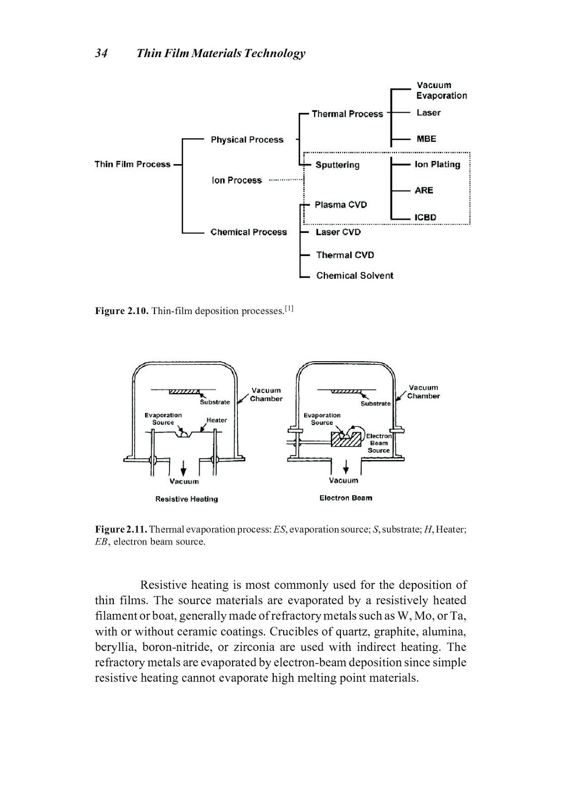
44-57 THIN FILM DEPOSITION PROCESS
-------------------------------------------------------------------------------------------------------------------
-------------------------------------------------------------------------------------------------------------------
-------------------------------------------------------------------------------------------------------------------
-------------------------------------------------------------------------------------------------------------------
K. Wasa, M. Kitabatake, H. Adachi, Thin Film Materials Technology: Sputtering of Compound Materials, Elsevier Science, 2004. https://books.google.fr/books?id=pmpV4RYHpdcC. Page 200-227; 59-60; 44-57.
----------------------------------------------------------------
Luminescent Materials and Applications
252-253 Sputter deposition
-------------------------------------------------------------------------------------------------------------------
-------------------------------------------------------------------------------------------------------------------
-------------------------------------------------------------------------------------------------------------------
A. Kitai, Luminescent Materials and Applications, Wiley, 2008. https://books.google.fr/books?id=yLy07tnBZ90C. Page 252-253.
-------------------------------------------------------------------
Solution Processing of Inorganic Materials
71 Summary of Film Deposition Methods
-------------------------------------------------------------------------------------------------------------------
-------------------------------------------------------------------------------------------------------------------
-------------------------------------------------------------------------------------------------------------------
-------------------------------------------------------------------------------------------------------------------
D. Mitzi, Solution Processing of Inorganic Materials, Wiley, 2008. https://books.google.fr/books?id=gQ9VFEsS8-kC. Page 71.
--------------------------------------------------
Practical Electronics for Inventors
483-485 Electronic Symbols
-------------------------------------------------------------------------------------------------------------------
-------------------------------------------------------------------------------------------------------------------
P. Scherz, Practical Electronics for Inventors,
McGraw-Hill, 2000. https://books.google.fr/books?id=HuPJqvWtedcC. Page 483-485.